Overview
In this series of posts I will explore controlling an Adafruit LED matrix with an FPGA using Verilog. The Adafruit LED matrix is similar to other available LED matrices floating around that use a shift register/output register combo. This makes them an ideal target for being controlled by an FPGA. Documentation on the hardware of these LED matrix boards seem to be sparse, so in this post I will try to explain the hardware as much as possible (to the best of my understanding).
Hardware
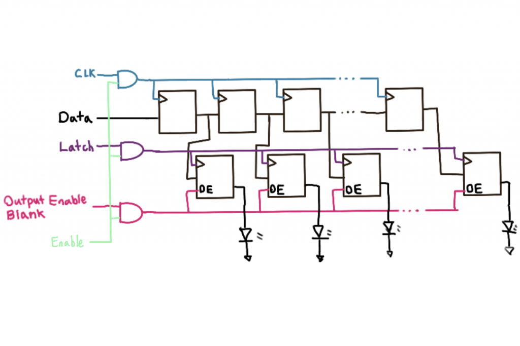
Each row of LEDs is controlled by three sets of output and shift registers (one each for red green, and blue). The shift register chain length is dependent on how wide the LED matrix is (so 32 wide = chain of 32 registers and 64 wide = chain of 64 registers). You can increase the length of this register chain by chaining together individual LED boards. The matrices will control/address two rows of these LEDs at a time.
Pinout
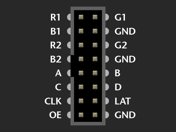
This is the pinout for a 32 row Adafruit LED matrix. Each of the R, G, and B signals hooks up to the data input of a shift register chain. The CLK, LAT, and OE signals hookup to the clock, latch, and output enable (aka blank) signals respectively. The A, B, C, and D signals are inputs to a decoder that output the enable signals for the register chains (in order to address them). The four bit address will address two rows at a time. For example, an address of 0000 would address the first and the sixteenth row, 0001 would address the second and seventeenth rows, etc.
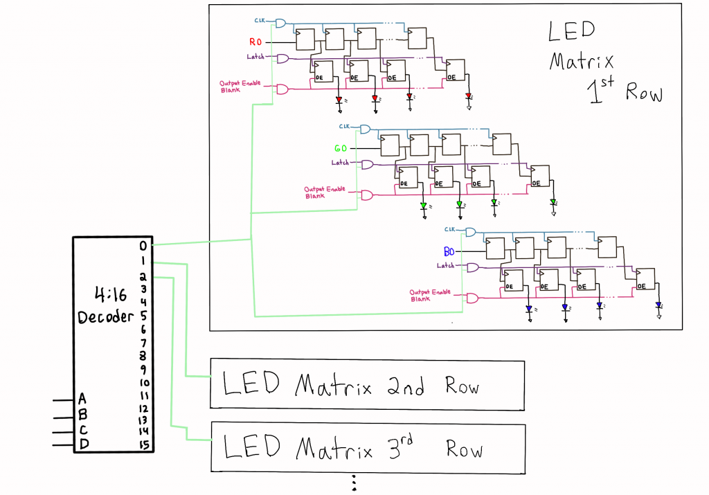
32 Row Matrix
This is what the hardware of what a 32 row LED matrix looks like including the four to sixteen decoder and the pinout signals. (Pins R1, G1, and B1 hook up to an identical set of the same hardware controlling rows 16 through 32 of the matrix).
16 Row Matrix
In a 16 row LED matrix the decoder would only accept a 3 bit input/address meaning the two copies of the hardware to the left would address rows 1-8 and 9-16.
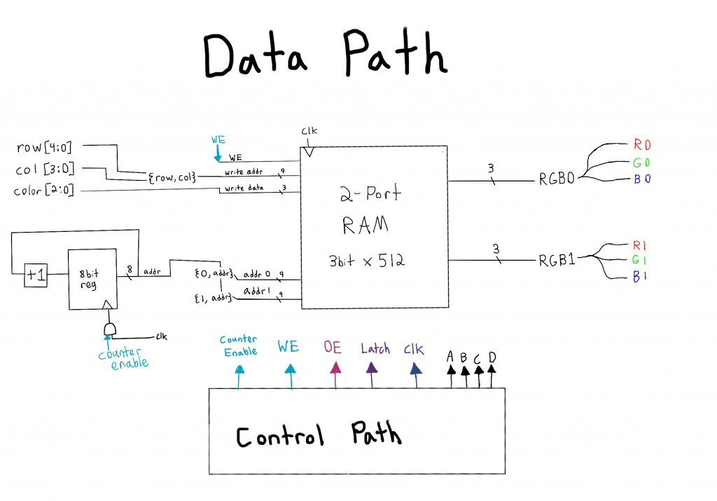
Datapath
Pictured is a bare bones data-path that could be used in an FPGA to drive the matrix (I will start out driving a 32×16 matrix and potentially modify this to drive a 64×32 matrix). The two port RAM acts as storage for the colors of each of the pixels in the matrix. This data-path supports three bit color, but could be expanded latter to support a greater variety of colors by PWMing the output.
In the next post I will explore what the control path would look like as well as beginning some Verilog code to create the data/control path designs.