In this post, I improve upon the data-path from the last post, design a control path, and write some Verilog to synthesize these designs for an FPGA.
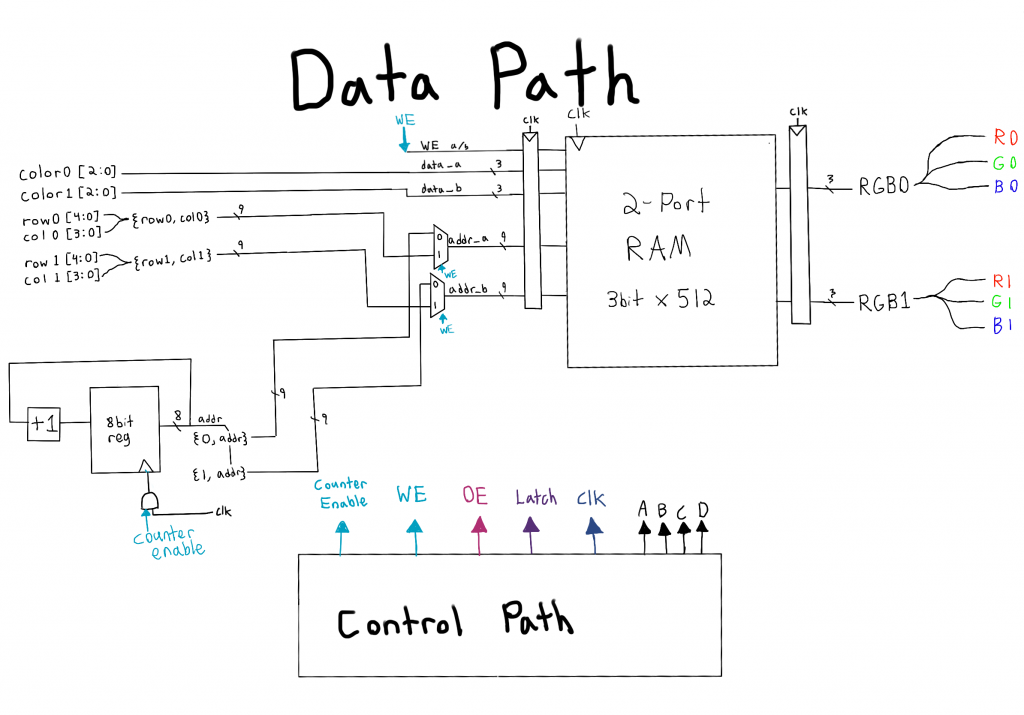
Data Path
This new data-path includes a more realistic model of what the on-chip RAM of the FPGA will look like. I will be utilizing an Altera (Intel) Cyclone FPGA, and the RAM will be pipelined and have 2 ports that share the read and write functionality. Since the 2 ports are shared for reading and writing a pair of multiplexers chooses between read and write addresses based on the value of the write enable signal (WE).
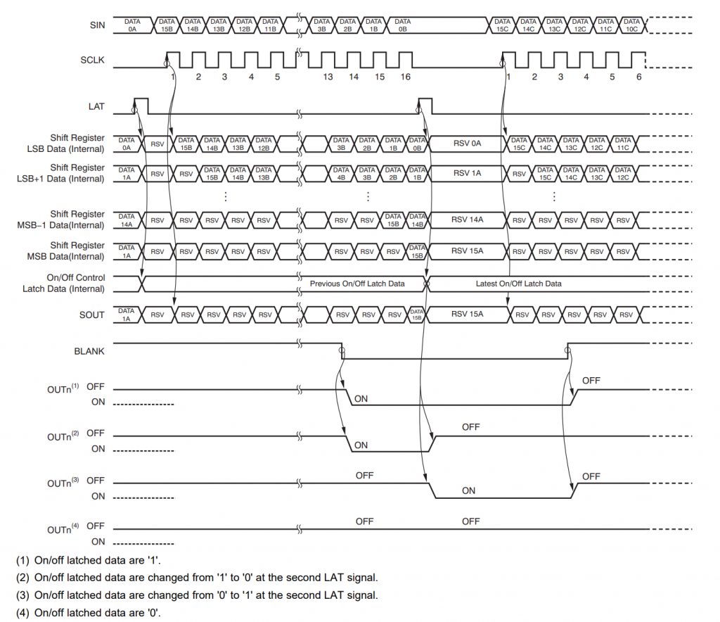
More Hardware
The best specifications I could find on the chip used in the LED matrix (including timing requirements, waveforms, etc) is a data sheet for a TI chip called the TLC59281 and a datasheet for an ON chip called the CAT4016. The chip that is built into my board is called “JX15020GP”, however, I’m pretty sure that this chip is very similar or a clone of the two chips mentioned above. Therefore the datasheets for these chips should give us a general idea of the timing requirements for the LED matrix.
I used the timing diagrams found in the data sheets to help determine states and the number of cycles spent in each state for the state machine in the control path.
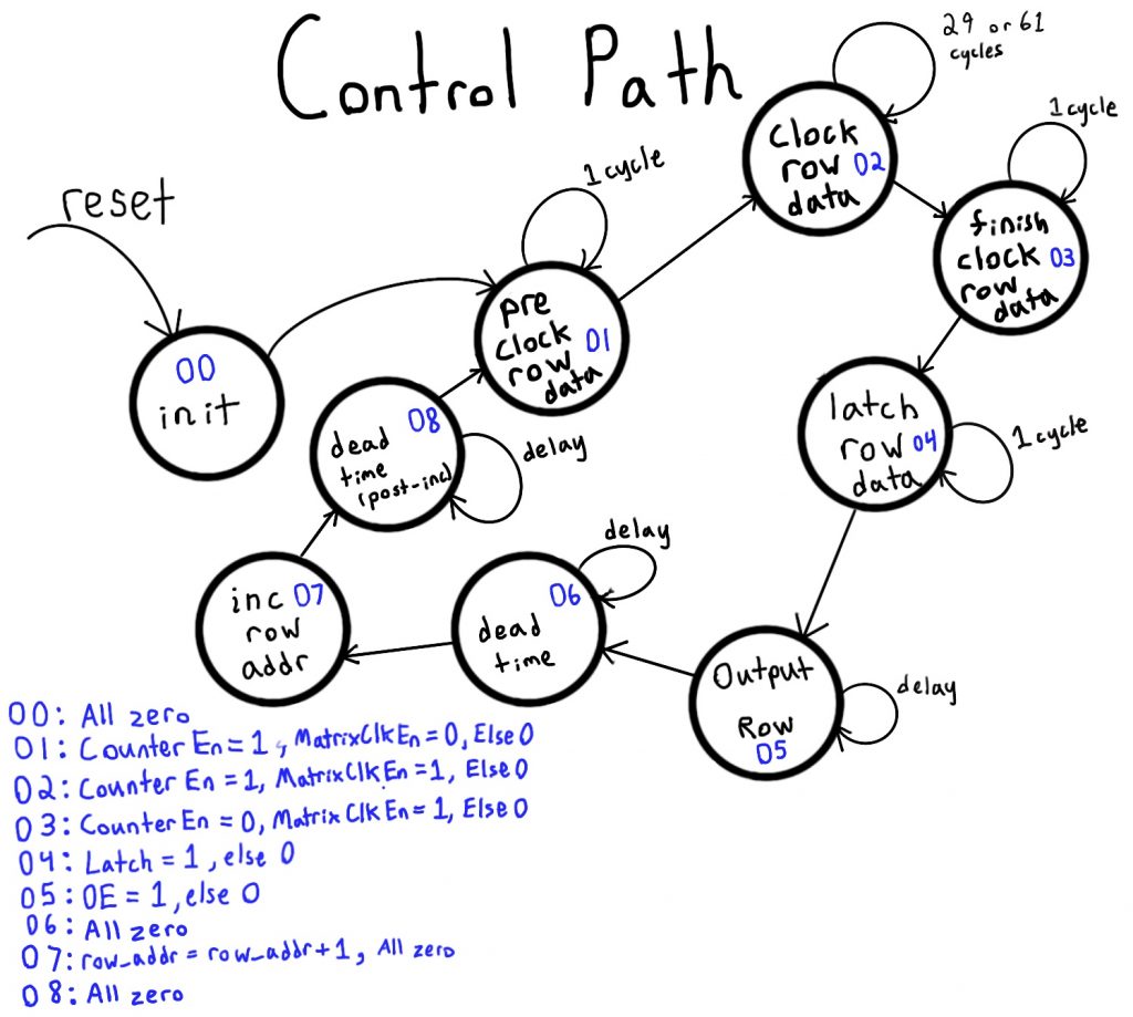
Control Path
The control path consists of 9 states. The init state is the state entered after a reset. The three states: pre-clock-row-data, clock-row-data, and finish-clock-row-data, are used to clock data into the LED matrix’s shift registers. These three states also compensate for the pipelining within the on-chip RAM (see data-path). After data has been clocked out, the latch-row-data state outputs a latch signal to latch the data to the LED matrix’s output register. Then, the output row state enables the output from the output registers to the LEDs. Finally, the inc-row-addr state increments the row address to allow the process to start again on the next set of rows. In between the output and increment states and the increment and pre-clock, are states that disable the LEDs. These “dead” states are used to allow the capacitances built up in the system to dissipate thereby reducing issues with ghosting.
Data Path Verilog
module led_matrix_data_path(
	input CLK,
	input RESET,
	input CE,
	input WE,
	input [4:0] row0,
	input [3:0] col0,
	input [2:0] color0,
	input [4:0] row1,
	input [3:0] col1,
	input [2:0] color1,
	output [2:0] RGB0,
	output [2:0] RGB1
	);

	reg [7:0] addr;
	always @(posedge CLK, posedge RESET) begin
		if(RESET) begin
			addr <= 0;
		end
		else if(CE) begin
			addr <= addr + 8'b1;
		end
		else begin
			addr <= addr;
		end
	end

	two_port_ram color_matrix(
		.reset(RESET),
		.address_a((WE) ? {row0,col0} : {1'b0, addr}),
		.address_b((WE) ? {row1,col1} : {1'b1, addr}),
		.clock(CLK),
		.data_a(color0),
		.data_b(color1),
		.wren_a(WE),
		.wren_b(WE),
		.q_a(RGB0),
		.q_b(RGB1)
	);
endmodule
This Verilog code implements the data-path seen above. It consists of a RAM whose addresses are provided by a register that increments when CE (count-enable) is high. Additionally, the RAM can be written to on both of its ports when it isn’t being read from. These times when the RAM can be written are determined by the control path. The row, col, and color inputs allow 2 pixels to be changes per clock cycle.
Model RAM Verilog (to be replaced with on-chip RAM)
module two_port_ram(
	input reset,
	input [8:0] address_a,
	input [8:0] address_b,
	input clock,
	input [2:0] data_a,
	input [2:0] data_b,
	input wren_a,
	input wren_b,
	output [2:0] q_a,
	output [2:0] q_b
	);

	reg [8:0] address_a_pipe;
	reg [8:0] address_b_pipe;
	reg [2:0] data_a_pipe;
	reg [2:0] data_b_pipe;
	reg wren_a_pipe;
	reg wren_b_pipe;

	reg [2:0] mem [511:0];

	reg [2:0] q_a_pipe;
	reg [2:0] q_b_pipe;
	integer i;

	always @(negedge clock) begin
		if(reset) begin
			address_a_pipe <= 0;
			address_b_pipe <= 0;
			data_a_pipe <= 0;
			data_b_pipe <= 0;
			wren_a_pipe <= 0;
			wren_b_pipe <= 0;
			q_a_pipe <= 0;
			q_b_pipe <= 0;
			for(i = 0; i < 512; i = i + 1) begin
				mem[i] <= 3'b000;
			end
			mem[0] <= 3'b000;
			mem[1] <= 3'b001;
			mem[2] <= 3'b010;
			mem[3] <= 3'b011;
			mem[4] <= 3'b100;
			mem[5] <= 3'b101;
			mem[6] <= 3'b110;
			mem[7] <= 3'b111;
		end
		else begin
			address_a_pipe <= address_a;
			address_b_pipe <= address_b;
			data_a_pipe <= data_a;
			data_b_pipe <= data_b;
			wren_a_pipe <= wren_a;
			wren_b_pipe <= wren_b;
			q_a_pipe <= mem[address_a_pipe];
			q_b_pipe <= mem[address_b_pipe];
		end
	end

	assign q_a = q_a_pipe;
	assign q_b = q_b_pipe;

endmodule
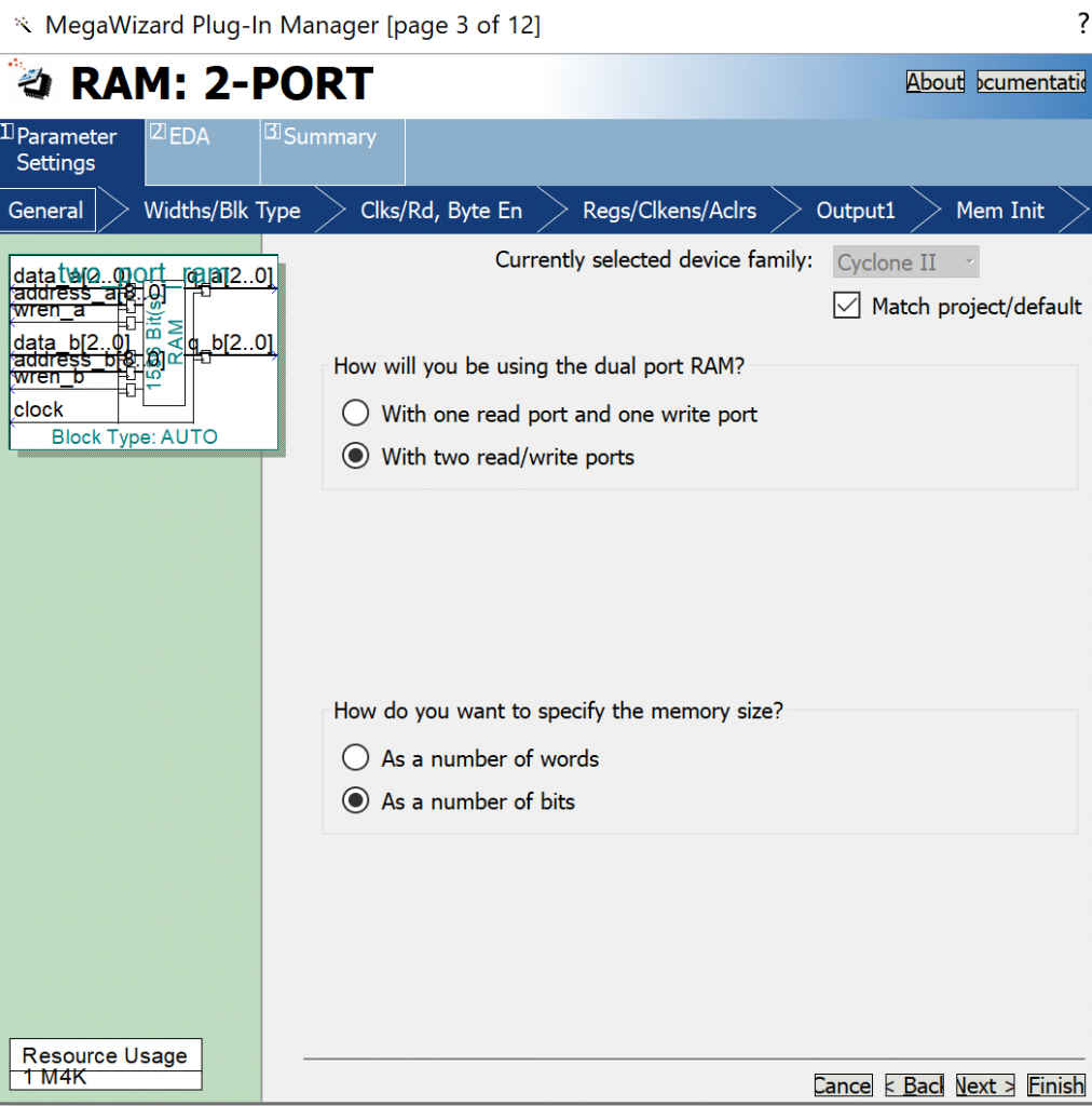
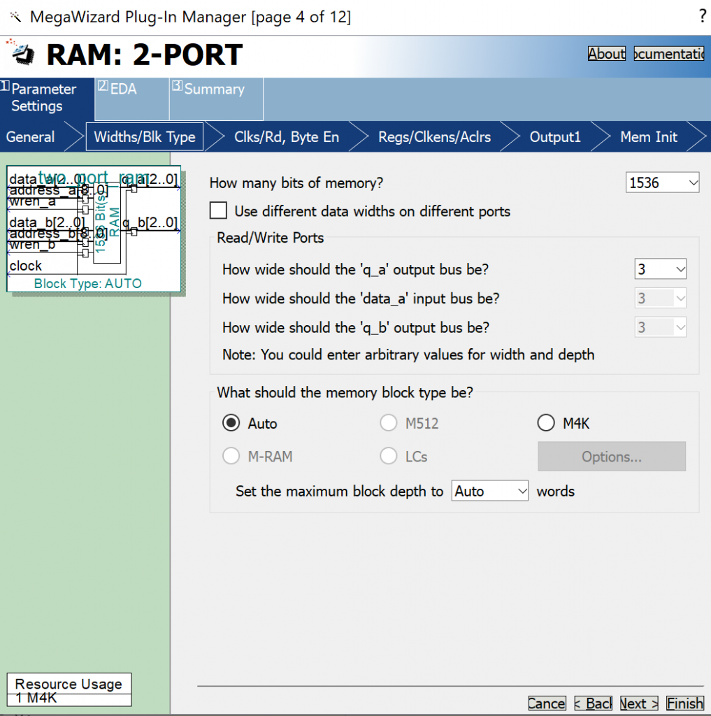
This is a Verilog model of a two-port RAM. Depending on the FPGA you are using you can leave this as is or replace it with an on-chip RAM. I am going to use an Altera Cyclone II FPGA to drive this LED Matrix. The editor for this FPGA: Quartus II 13.0sp, can allow you to use on-chip 2 port RAM via its “MegaWizard Plug-In Manager”. By using the Memory Compiler option and selecting a two-port RAM that has a bit width of 3 bits and a size of 1,536 bits an on-chip RAM that is functionally equivalent to the model can be used.
Control Path Verilog
module led_matrix_ctrl_path(
input CLK,
input RESET,
output reg CE,
output reg CLK_EN,
output reg LAT,
output reg OE,
output reg busy,
output reg [2:0] row_addr
);

parameter INIT = 4'd0, PRE = 4'd1, DATA = 4'd2, POST = 4'd3,
LATCH = 4'd4, OUTPUT = 4'd5, DEAD = 4'd6, INC = 4'd7, DEADinc = 4'd8;

reg [31:0] cycle_count;
reg [3:0] state;
reg [3:0] next_state;
//Next State Logic
always @ (*) begin
case(state)
	INIT:   next_state = PRE;
	PRE:    next_state = (cycle_count == 1) ? DATA : PRE;
	DATA:   next_state = (cycle_count == 29) ? POST : DATA;
	POST:   next_state = (cycle_count == 1) ? LATCH : POST;
	LATCH:  next_state = OUTPUT;
	OUTPUT: next_state = (cycle_count == 15000) ? DEAD : OUTPUT;
	DEAD:   next_state = (cycle_count == 250) ? INC : DEAD;
	INC:    next_state = DEADinc;
	DEADinc:next_state = (cycle_count == 250) ? PRE : DEADinc;
	default: next_state = INIT;
endcase
end

//Output Logic
always @ (state) begin
	case(state)
	INIT:   begin CE = 1'b0; CLK_EN = 1'b0; LAT = 1'b0; OE = 1'b1; busy = 0; end
	PRE:    begin CE = 1'b1; CLK_EN = 1'b0; LAT = 1'b0; OE = 1'b1; busy = 1; end
	DATA:   begin CE = 1'b1; CLK_EN = 1'b1; LAT = 1'b0; OE = 1'b1; busy = 1; end
	POST:   begin CE = 1'b0; CLK_EN = 1'b1; LAT = 1'b0; OE = 1'b1; busy = 1; end
	LATCH:  begin CE = 1'b0; CLK_EN = 1'b0; LAT = 1'b1; OE = 1'b1; busy = 0; end
	OUTPUT: begin CE = 1'b0; CLK_EN = 1'b0; LAT = 1'b0; OE = 1'b0; busy = 0; end
	DEAD:   begin CE = 1'b0; CLK_EN = 1'b0; LAT = 1'b0; OE = 1'b1; busy = 0; end
	INC:    begin CE = 1'b0; CLK_EN = 1'b0; LAT = 1'b0; OE = 1'b1; busy = 0; end
	DEADinc:begin CE = 1'b0; CLK_EN = 1'b0; LAT = 1'b0; OE = 1'b1; busy = 0; end
	default:begin CE = 1'b0; CLK_EN = 1'b0; LAT = 1'b0; OE = 1'b1; busy = 0; end
endcase
end

//State Transition Logic
always @ (posedge CLK, posedge RESET) begin
	if(RESET) begin
		state <= INIT;
		cycle_count <= 0;
	end
	else if(next_state != state) begin
		state <= next_state;
		cycle_count <= 0;
	end
	else begin
		state <= next_state;
		cycle_count <= cycle_count + 1;
	end
end

//Row Address Logic
always @ (posedge CLK, posedge RESET) begin
	if(RESET) begin
		row_addr <= 0;
	end
	else if(state == INC) begin
		row_addr <= row_addr + 1;
	end
	else begin
		row_addr <= row_addr;
	end
end
endmodule
The control path is implemented as a Verilog state machine that is broken into switch statements that implement the next state logic, output logic, and transition logic.

Each state in the control path FSM has a corresponding parameter in the Verilog and the “cycle_count ==” in each case of the next state logic determines how many cycles are spent in each state. The cycle_counts for the PRE, DATA, and POST states are determined by the data-path pipeline and the amount of data to be clocked out. The cycle_counts for the OUTPUT and DEAD states were determined by trial and error (the delays that resulted in most brightness, greatest frame-rate, and least ghosting) these values may vary from matrix to matrix based on the matrix’s chip’s timing requirements.
Top Level (plugs into LED Matrix)
module top_level(
	input CLK,
	input reset,
	output clk_out,
	output [2:0] RGB0,
	output [2:0] RGB1,
	output LAT,
	output OE,
	output [2:0] led_addr,
	output [3:0] gnd
);

wire CE;
wire CLK_EN;
wire WE;
wire RESET;
reg CLK_SLO;
assign RESET = ~reset;
assign clk_out = CLK_EN & CLK_SLO;
assign gnd = 4'b0000;

//Clock Divider (50 MHz -> 25Mhz)
always @(posedge CLK, posedge RESET) begin
	if(RESET) begin
		CLK_SLO <= 0;
	end
	else begin
		CLK_SLO <= ~CLK_SLO;
	end
end

led_matrix_data_path data_path(
		.CLK(CLK_SLO),
		.RESET(RESET),
		.CE(CE),
		.WE(1'b0),
		.row0(5'b00000),
		.col0(4'b0000),
		.color0(3'b000),
		.row1(5'b00000),
		.col1(4'b0000),
		.color1(3'b000),
		.RGB0(RGB0),
		.RGB1(RGB1)
);

led_matrix_ctrl_path ctrl_path(
	.CLK(CLK_SLO),
	.RESET(RESET),
	.CE(CE),
	.CLK_EN(CLK_EN),
	.LAT(LAT),
	.OE(OE),
	.busy(busy),
	.row_addr(led_addr)
);
endmodule
The top-level is mapped to output pins on your FPGA using your FPGA software’s pin planner. The corresponding pins on the FPGA can then be wired to the pin-out of the LED Matrix.
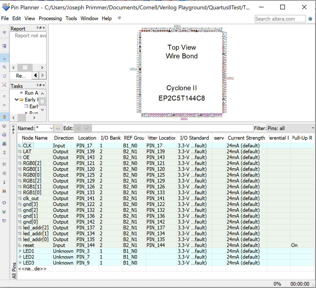
According to both chips discussed above, the TI chip max clock rate was 35MHz and the ON chip was 25MHz. Therefore, in order to meet the timing requirements, a clock divider is used to bring the clock rate down from 50MHz to 25MHz. For now, we will tie the writing functionality of the RAM to all zeros.
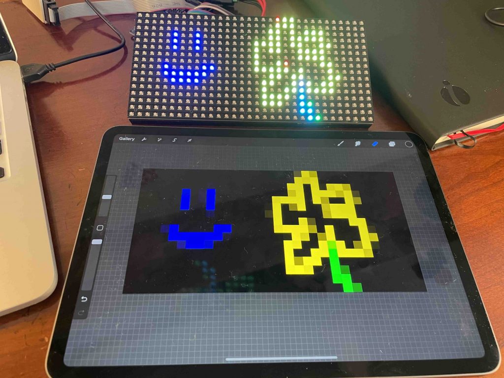
The RAM of the FPGA can be initialized using a memory file (mif). By setting the color values of the pixels of the LED matrix in this file, pictures can then be drawn.
In the next post, I will explore using the writing functionality of the RAM to animate interesting patterns on the LED matrix.